
Assembly and characterization of carbon nanotube biosensors on integrated circuits
Former Unit Leader Urs Frey and his team describe the technology developed at QBiC.
Mar 23, 2017 Tweet
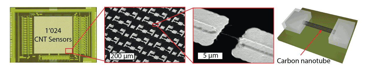
Micrograph of the CMOS system with the CNT sensors in the center (left). Scanning electron micrograph of the CNT sensor array. The sensor pattern can be seen at medium magnification (200 µm scale bar). At higher magnification, the two levels of Pt can be seen, and a CNT bundle between the electrodes becomes visible (5 µm scale bar). Illustration of a single CNT sensor (right).
Nanomaterials, such as carbon nanotubes (CNTs), are promising candidates as sensing elements for the detection of chemical and biological species, due to their high surface-to-volume ratio and unique electrical properties. When integrated at a large scale into electronic systems, highly sensitive, label-free electrical detection can be achieved. However, such integration is still very challenging, due to inherent material properties and limitations of the industrial processes used to fabricate standard electronic systems. To overcome this limitation, first author Florent Seichepine and colleagues developed a reliable fabrication processes for the deposition of CNTs onto a CMOS microsystem[1].
CMOS, or complementary metal–oxide–semiconductor, is the most common technology used for the construction of integrated circuits, such as microprocessors, memory, image sensors, data convertors, etc. CMOS technology allows for the integration of complex electronic functions into very small pieces of silicon. When used for sensor systems, CMOS allows amplification and multiplexing sensor signals right at the source. This in turn keeps noise interference at a minimum and it also allows integrating thousands or even millions of sensing elements on a very small area. In the context of this work, CMOS was critical to achieve a highly-multiplexed sensing platform with 1024 sensors and to amplify and transmit the minute electrical signals from the CNTs to personal computers for further analysis.
CNTs, or carbon nanotubes, were discovered by Sumio Iijima and since have been studied for their outstanding mechanical and electronic properties. Especially their inert nature and high surface-to-volume ratio render them an ideal material to detect biological species. Recently, it has been shown that CNTs can be used as sensors to detect single DNA molecules or even conformation changes of proteins attached to their surfaces. Furthermore, by functionalizing their surface with specific receptors, such as antibodies or single strained DNA, CNTs sensors can be tuned to detect specific biomolecules at very low concentrations. This offers the possibility to detect low concentrations in real time without target molecule amplification methods and without fluorescent labeling.
While previous work has demonstrated the outstanding sensing abilities of CNTs for biological species, it has been difficult to bring these properties into more widespread applications. Unfortunately, the high sensitivity of CNT sensors also entails the presence of baseline fluctuations due to unspecific and random adsorption events, which are likely to create detection errors. In addition, the limited adsorption area of single-CNT nanosensors leads to slow response times for low concentrations. Frey explains, “Both these limitations can be tackled by integrating large arrays of individually addressable sensor elements, as the total absorption area can be increased and statistical analysis methods can be applied to extract reliable detection information. Our work demonstrates that CNT sensors can indeed be integrated at a large scale in a reliable manner. The fabrication process we demonstrated could be used for the next generation of sensor devices, with applications in point-of-care diagnostics, for example.”
Frey describes how the research relates to the field, “Over the past decade, the development of new bioelectronics and biosensors based on CMOS technology enabled the study of neural networks at a completely new scale. Minute electric signal from axonal processes can now be tracked how they propagate from one neuron to the next. Now, with the emerging of new platforms integrating nanomaterials to probe chemical species it will soon be possible to study chemical signaling of complex biological systems. In systems, such as cultured neuronal networks, our technology may in future allow to record the chemical communication and local concentrations of molecules, such as neurotransmitters.”
Regarding the challenges of this project, he says, “The greatest challenge was the development of a technology to fabricate sensors at the nanoscale without the fabrication capabilities of a big, commercial CMOS foundry. Our choice to use dielectrophoresis (manipulation of particles using an electric field gradient) has been proven to be rewarding as we managed to optimize the process to reach an unexpectedly high yield of functional devices. This has been made possible by using the well-equipped micro-fabrication facilities of RIKEN QBiC and keeping an open mind to cope with the given fabrication limitations.” This work was done in the Frey Initiative Research Unit in Kobe, Japan.
- Seichepine F, Rothe J, Dudina A, Hierlemann A, Frey U (2017) Dielectrophoresis-assisted integration of 1024 carbon nanotube sensors into a CMOS microsystem. Advanced Materials doi: 10.1002/adma.201606852